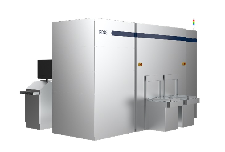
The
TRENG-PLP
Coater
The
Coater
enables
2.5D
packaging—a
next-generation
semiconductor
production
technology—to
be
applied
to
larger
substrates.
Specifically,
it
is
capable
of
creating
detailed
rewiring
layers
on
glass
substrates
for
use
in
interposers,
which
are
a
key
component
of
integrated
circuits.
In
this
way,
the
Coater
facilitates
the
production
of
high-performance
semiconductors.
Toray Engineering has already delivered pilot Coaters to a number of major semiconductor manufacturers to demonstrate its capabilities. Now, the company is preparing to mass-produce the devices, and is targeting orders totaling 3 billion yen by fiscal 2025, and 6 billion yen by fiscal 2030.
In recent years, increased demand for generative AI servers has resulted in a proliferation of hyperscale data centers. As semiconductor performance has improved, the market for high-performance semiconductors has expanded rapidly; at the same time, this technological progress has driven demand for larger-scale and more efficient advanced semiconductor packaging, which is indispensable for the production of advanced semiconductor devices.
Interposers are a key component in advanced semiconductor packaging, and are traditionally made of silicon. However, since interposers are square and silicon wafers are round in shape, cutting square interposers out of 300mm-diameter round silicon wafers inevitably results in waste silicon. Moreover, as semiconductor performance increases, package sizes have been increasing year on year, leading to fears of further decreases in production efficiency.
PLP technologies, which use 600mm-square glass substrates, are seen as a potential solution to the above problems. The larger area of the glass substrate means that larger-scale packages can be produced compared to what is possible with silicon wafers, while its square shape means that the entire substrate can be effectively used to create square interposers without resulting in unused substrate.
Yet the use of PLP technologies to create circuits is not without its own issues: warping of the glass substrate must be prevented, while the wiring materials and photoresist materials must be of a uniform thickness.
To prevent warping, Toray Engineering has developed new technologies for the handling of large glass substrates, drawing on proprietary coating technologies for LCD panels, which are capable of controlling thickness with a high degree of precision. These technologies enable the TRENG-PLP Coater to create high-density rewiring layers on 600mm-square glass substrates.
Hashtag: #toray #TRENG
The issuer is solely responsible for the content of this announcement.
Support InfoStride News' Credible Journalism: Only credible journalism can guarantee a fair, accountable and transparent society, including democracy and government. It involves a lot of efforts and money. We need your support. Click here to Donate
